Specification
| T5L1 ASIC | DWIN auto-disposito chip.Massa productio in MMXIX, A 600Mhz dua- core chip, GUI core et OS core, 1MBytes neque Flash in chip, 512KBytes ad usum datorum reponunt.Rewrite cyclum: per 100,000 tempora |
| Color | 16.7M(16777216)colores |
| LCD Type | IPS |
| Viewing Anglus | 85/85/85/85 (L/R/U/D) |
| Panel Type | IPS |
| Propono Area(AA) | 74.0mm (W) × 74.0mm (H) |
| Resolution | 720× 720 |
| Backlight | LED |
| splendor | 300nit |
| Potentia Voltage | 6~36V |
| Operatio Current | VCC = +12V, Backlight on, 175mA |
| VCC = +12V, Backlight off, 80mA |
| Operatio Temperature | -20~70℃ |
| Repono Temperature | -30~80℃ |
| opus Umor | 10%~90% RH |
| Baud rate | 3150~3225600bps |
| Output intentione | Output 1, Iout = 1mA;3.0~3.3 V |
| Output 0, Iout = -1mA;0~0.3 V | |
| Input intentione | Input 1, Iin = 1mA;2.4~5.0V |
| Input 0, Iin = -1mA;0~0.5V | |
| Interface | UART1: TTL |
| Socket | 50Pin-0.5mm FCC |
| USB interface | Ita |
| SD Slote | VERO (SDHC/FAT32 Format) |
| UI Version | TA/DGUSⅡ (DGUSⅡ praestructum) |
| Periphericum | Capacitive tactus panel, Buzzer |
| Dimension | 115.6mm (W) 95.8mm(H) 15.6m(T) |
| Net Pondus | 85g |
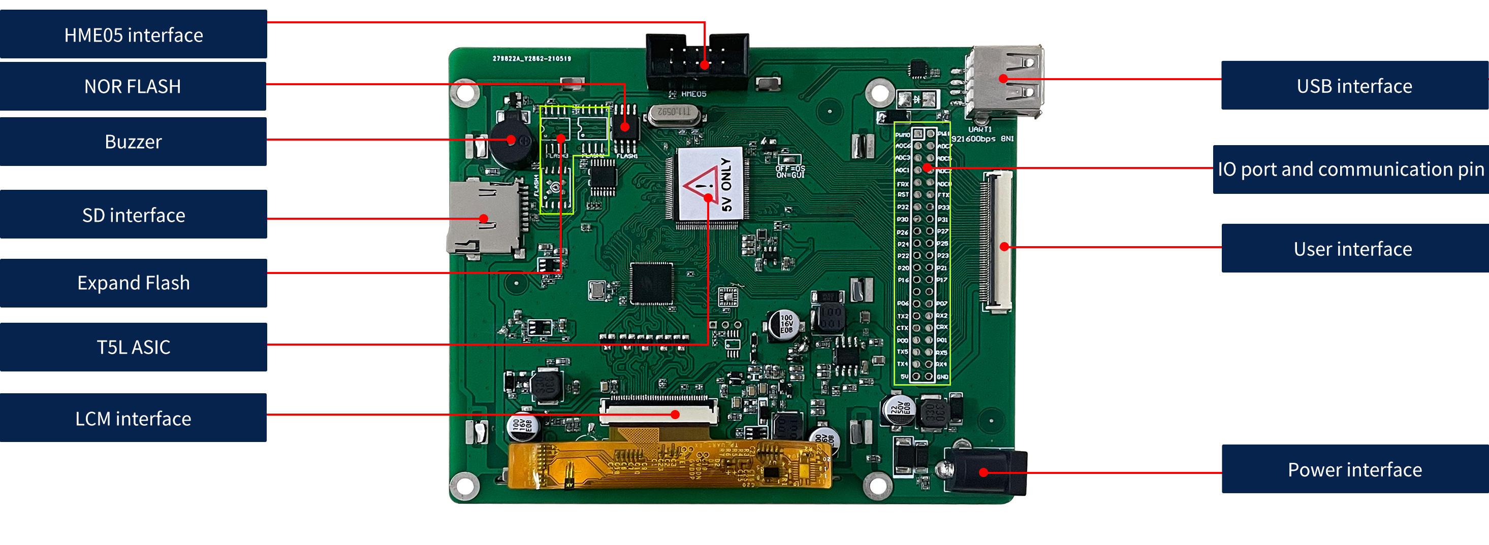
| 1# | JTAG interface, coniungere ad PGT05 (renovatio subesse) vel coniungere ad HME05 (emulationis debugging) |
| 2# | USB interface, coniungere ad UART1 |
| 3# | Expande Flash interface, quae dilatari potest ad 64 Mbytes NEC FLASH vel 48 MBYTES NEC FLASH+512 Mbytes NAND FULG.NAND FULGUR 4 situ solidari debet ut FULGUR |
| 4# | D card ardenti interface |
| 5# | 2.54mm per foramen caudex usorum interfacies ducit, 20 IO interfaces, 3 UART Vide portus, 1 portus CAN, 7 AD interfaces, 2 PWM interfaces |
| 6# | 6-36V ampla voltage potentia copia interface |
| PIN | Definition | Descriptio |
| 1# | GND | Commune |
| 2# | RX4 | UART4 data receptio |
| 3# | RX5 | UART5 Data receptione |
| 4# | P01 | I / O os |
| 5# | CRX | Potest interface notitia receptio |
| 6# | RX2 | UART2 notitia accepto |
| 7# | P07 | I / O |
| 8# | P15 | I / O |
| 9# | P17 | I / O |
| 10# | P21 | I / O |
| 11# | P23 | I / O |
| 12# | P25 | I / O |
| 13# | P27 | I / O |
| 14# | P31 | I / O |
| 15# | P33 | I / O |
| 16# | FTX | FSK transceiver data receptio |
| 17# | ADC0 | AD input |
| 18# | ADC2 | AD input |
| 19# | ADC5 | AD input |
| 20# | ADC7 | AD input |
| 21# | PWM1 | 16bit PWM output |
| 22# | 5V | potentia initus |
| 23# | TX4 | UART4 notitia tradenda |
| 24# | TX5 | UART5 notitia tradenda |
| 25# | P0.0 | I / O |
| 26# | CTX | Can notitia tradenda interface |
| 27# | TX2 | UART2 notitia tradenda |
| 28# | P06 | I / O |
| 29# | P14 | I / O |
| 30# | P16 | I / O |
| 31# | P20 | I / O |
| 32# | P22 | I / O |
| 33# | P24 | I / O |
| 34# | P26 | I / O |
| 35# | P30 | I / O |
| 36# | P32 | I / O |
| 37# | RSTN | Ratio reset initus |
| 38# | FRX | FSK transceiver notitia tradenda |
| 39# | ADC1 | AD input |
| 40# | ADC3 | AD input |
| 41# | ADC6 | AD input |
| 42# | PWM0 | 16bit PWM output |